-
Smallest silicon footprint per die.
-
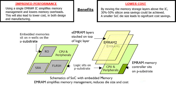
EMRAM is made up
of a memory controller and EMRAM storage elements. The controller is
integrated into the logic portion while the EMRAM storage elements are
built on top of the logic via a special metallization process.
- To increase memory capacity further, up
to 2 additional EMRAM storage layers can be added onto the basic EMRAM
IC.-
Does not require n-wells on p-substrates
-
Different from other embedded memories that require n-wells on a
p-substrate, EMRAM is made up of metallic layers that sit on top of the
memory controller (psubstrate).-
Short
manufacturing cycle
- As the EMRAM controller is
integrated into the logic, only additional time required to complete
the EMRAM storage layers is less than 3 days.
|
-
Compatible with CMOS, BiPolar, GaAs, SOI and more
-
One EMRAM replaces ROM, SRAM, DRAM, EEPROM and FLASH
-
Very fast Read & Write
- Write less than 2ns. Cycle time 50ns.
Non-volatile, excellent data storage endurance
-
EMRAM is non-volatile, and retains data ad infinitum.
Read/Write endurance
- With an infinite endurance theoretically, EMRAM has demonstrated
endurance of more than 1015
read / write cycles.
Elevated temperature endurance
- EMRAM storage layers are stable beyond 300˚C with
compatible silicon substrates.
Low power
Radiation hardened
|

